FPGA: UART
Now that we have a FPGA add in card, we can start to prototype some hardware using this FPGA. The FPGA we got has 15k logic elements, this should be plenty for us to implement many features at once.
One of the first feature I’d like to implement is a reliable UART/serial communication card.
Breakdown of the UART Controller
- Parallel to serial converter (UART Tx side)
- Serial to parallel converter (UART Rx side)
- Interface with S100 Bus
- Control / Data registers for the serial
Implemeting the serial Tx side
The goal here is to implement a TTL UART transimitter. TTL UART is rather simple to implement, the line toggle once per bit (at the bit rate frequency). The line normally idle at high logic level, and drops down for 1 cycle (1 start bit), then send the 8 bits followed by 1 cycle high (stop bit). This can be implemented by a simple state machine.
You can find the implementation code here.
The module is designed so that the transimitter can run at a different clock than the control interface module. This is important, because very likely the bitrate of the UART will not be the clock speed at which the majority of the design will be running at. The CDC(clock domain crossing) is handled by using a hand-shake method.
The controller can simply put the data on the bus, then signal the wr (write) wire. The data / write can be deasserted as soon as the tx module respond with the ack signal. After detecting the ack signal, the master can assert the ack_clr signal to show that it has recieved the ack. The tx module then becomes ready to recieve the next byte.
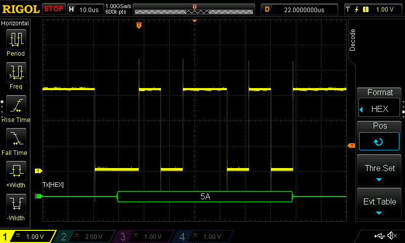
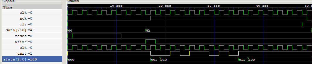
This can be seen from the following simulation capture showing the transimitter
sending an ‘0x5A’ byte. (The yellow waveform is the TTL serial).
Also the module work on real hardware, here’s a scope capture of it sending the same ‘0x5A’ byte at 115200 baud.